
Chemical Vapor Deposition Overview
Chemical vapor deposition (CVD) enables high quality thin film deposition by transporting gaseous precursors into a heated reaction chamber containing the target substrate. Within the chamber, the volatile precursors decompose and react at the substrate's surface, forming a uniform thin film coating while producing volatile byproducts. The byproducts and any unreacted precursors exit the chamber as exhaust. CVD can deposit many materials, including silicon for photovoltaics, by carefully selecting precursor chemistry. The technique provides excellent thickness and composition control but requires high temperatures. Overall, CVD's versatile thin film fabrication makes it ideal for manufacturing advanced solar cell designs.
Comparing Hot Wall and Cold Wall Reactors for Chemical Vapor Deposition
Hot Wall Reactors
Hot wall CVD reactors promote uniform coatings by heating the entire chamber, allowing large batch processing. However, high thermal mass prolongs heating, wasting significant energy. Coating on chamber walls complicates cleaning. Moreover, the all-encompassing heat triggers gas phase reactions producing lower quality films. In contrast, cold wall CVD selectively heats only the substrate surface via lamps or RF induction. This targeted approach enables rapid heating, reduces gas reactions, and localizes deposition, enhancing control. Though batch sizes are smaller, cold wall CVD improves efficiency, cleanliness, and coating quality.
Cold Wall Reactors
Unlike hot wall reactors, cold wall CVD systems selectively heat only the substrate by lamps or radio frequency induction while cooling the chamber walls. Concentrating heat on the deposition surface enables compound semiconductor processes requiring high temperatures. By localizing thermal energy, cold wall reactors enhance efficiency, reduce gas phase reactions, and limit deposition to the target substrate.
Offering precise temperature control, cold wall CVD confines heating to only the target substrate, enabling fast deposition rates without superfluous chamber wall coatings. Lower thermal mass slashes energy consumption while localized deposition prevents wasteful gas phase reactions. However, the selective substrate heating requires more complex operation and limits batch sizes. Non-uniform heating can also cause uneven coating thickness. Overall, cold wall CVD promotes efficiency and film quality despite higher complexity and lower throughput compared to hot wall systems. For processes demanding stringent parameters like semiconductor manufacturing, cold wall reactors provide superior performance.
Types of Chemical Vapor
Plasma-enhanced Chemical Vapor Deposition
Unlike standard CVD, plasma-enhanced chemical vapor deposition (PECVD) activates precursor gases into reactive plasma. By applying radio frequency or direct current discharge between two electrodes, the gases passing through the chamber transform into ionized plasma. This plasma reacts readily with chamber surfaces, allowing PECVD to operate at lower temperatures while still depositing high quality thin films. The lower thermal budget expands material options.
Thermal Chemical Vapor Deposition
Thermal CVD, or open-air CVD, involves highly reactive precursors from mixing precursor materials into combustible gases. The enhanced reactivity enables thin film deposition to occur on substrates under open atmosphere conditions without a vacuum chamber. This simplifies the coating process.
Hot-filament Chemical Vapor Deposition
Hot filament chemical vapor deposition (HFCVD) utilizes a heated filament to decompose precursor gases before reaching the relatively cooler substrate. The filament catalyzes the reactions, allowing depositions at lower substrate temperatures. This enables coating heat-sensitive materials like plastics.
Metalorganic Chemical Vapor Deposition
In metalorganic chemical vapor deposition (MOCVD), metalorganic precursors like germane and arsine undergo chemical reactions to deposit epitaxial thin films. Unlike molecular beam epitaxy which utilizes physical deposition, MOCVD relies on gas phase chemistry. The technique produces high quality single crystal or polycrystalline films. Common applications include LEDs, laser diodes, and advanced solar cells.
Laser Chemical Vapor Deposition
Laser chemical vapor deposition (LCVD) enables precise localized depositions by using a laser to selectively heat areas of the substrate, accelerating deposition on the irradiated spots. Scanning the laser rapidly coats patterns without masks. The technique allows "direct writing" of semiconductors and other thin film materials in a simple, flexible manner.
Advantages of Chemical Vapor Deposition for Thin Film Fabrication
l Cost-effectiveness - CVD provides high quality coatings at relatively low costs compared to other methods.
l Versatility - The technique can deposit a wide array of materials including metals, alloys, semiconductors, nitrides, oxides, and more.
l Rapid deposition - CVD often enables very high growth rates up to 100 microns per hour while maintaining strong adhesion.
l Uniformity - Gas precursors permeate trenches and voids, allowing highly conformal coatings of uniform thickness even on complex geometries.
l Purity - Carefully controlled precursor chemistry results in films with low contaminants and high purity essential for many applications.
l Conformality - The gas phase process coats non-line-of-sight and three dimensional surfaces uniformly.
Overall, CVD offers a flexible, affordable thin film deposition method capable of high purity, uniformity, and speed at scale. These advantages drive its ubiquity across microelectronics, solar cells, and other advanced technologies.
The Versatility of Chemical Vapor Deposition for Advanced Materials Fabrication
l Semiconductor fabrication - CVD is widely used to deposit thin films of silicon, silicon dioxide, silicon nitride, and other materials for integrated circuits, transistors, solar cells, and LEDs.
l Coating of tools and machine parts - CVD forms wear-resistant coatings of titanium nitride, titanium carbide, zirconium nitride, and other ceramics on cutting tools, medical implants, and aerospace components
l LED and laser diodes - CVD is used to deposit layers of gallium nitride, gallium arsenide, and related materials for light-emitting diodes and diode lasers.
l Data storage - CVD deposited layers are used in the production of hard disks, magnetic recording heads, and optical discs.
l Corrosion and oxidation resistance - CVD coatings of aluminum oxide, silicon carbide, chromium, and other materials provide protection from corrosion, weathering, and high temperatures
l Optical coatings - CVD creates specialized anti-reflective coatings, reflective layers, and optical filters from materials like silicon oxide for lenses and other optical devices.
l MEMS and NEMS - CVD is important for depositing thin films for microelectromechanical (MEMS) and nanoelectromechanical (NEMS) devices.
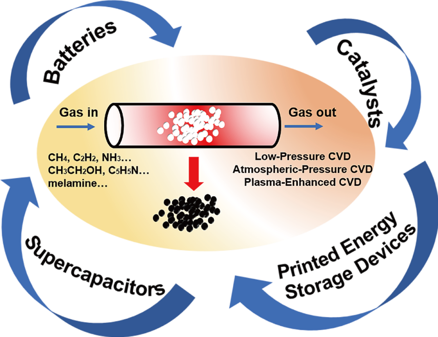
l Carbon nanomaterials - CVD enables controlled growth of carbon nanotubes, graphene, and diamond films.
Conclusion
Providing versatile coatings across industries, chemical vapor deposition delivers numerous advantages from its superior control over film uniformity, purity, and composition. Further innovations will unlock its full potential.