Challenges for Thin Film Coating in the Development of Semiconductors
From both technological and economic perspectives, semiconductors play an enormous role in today's society. Nearly all electronic products, such as computers, mobile phones, and digital recorders, have a close relationship with semiconductors. However, as the semiconductor market continues to grow rapidly, it faces several challenges that need to be addressed.
Challenges for today
Firstly, with the increasing number of devices connecting to and thriving on the Internet of Things (IoT), there is a growing demand for wireless connectivity and faster data transfer speeds. Semiconductor chips need to meet these requirements to ensure seamless integration and efficient communication.
Secondly, consumers have a strong preference for water-resistant or waterproof mobile devices. This poses a challenge for semiconductor suppliers to develop coatings that protect the chips from moisture and ensure their reliability and durability.
Thirdly, devices need to withstand constant, prolonged use and occasional rough handling. Semiconductor chips must be able to endure these conditions without compromising their performance or reliability.
Thinfilm coating and semicon industry
Thin film coating significantly impacts the semiconductor industry. Specifically, due to small component sizes, manufacturing cannot individually install each part like machines. Instead, similar printing deposits layers actively. Stacking materials in this way creates desired circuits precisely at the microscopic scale.

Moreover, this process demands advanced design talents. Additionally, accurate manufacturing techniques prove necessary. Furthermore, thin film techniques like sputtering and chemical vapor deposition deposit various materials onto silicon substrates. Thin film coating represents an indispensable production step for semiconductor chips by layering different materials. It actively stacks microscopic parts through printing-like layering rather than manual assembly. In conclusion, precise design and deposition build integrated circuits from the bottom-up on wafers through thin film methods.
Future
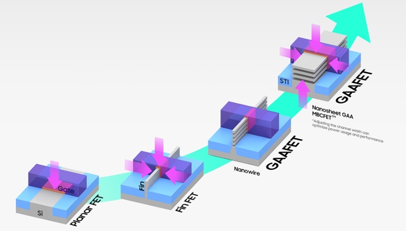
Looking ahead, thin film coating in semiconductor development faces two primary challenges. Firstly, performance improvement remains necessary. Specifically, materials like aluminum, copper, and molybdenum now purify further. Additionally, sputtering processes sharpen in precision. These advancements enable production reaching as small as 3nm by 2023. Such refined deposition and processes actively utilize more advanced technologies. As a result, smaller, intricate chips emerge with boosted performance.

Secondly, focus directs to lengthening semiconductor lifespan. Most naturally experience limited lifetime due to wear mechanisms. Defects within active areas significantly reduce life, especially with high currents and heat. Applying a coating helps actively prolong circuit viability. Appropriate coatings protect drive circuitry and frames against corrosion. The coating serves as an effective barrier deterring contaminants. Moreover, it protects integrity from potential issues like tin whiskers through preservation. This extends semiconductor operation without damage from the operating environment.

As an important supplier of sputter targets and other coating materials, QS Advanced Materials Inc is committed to meeting the needs of customers in the semiconductor industry. We can produce the desired materials in a short period according to customer requirements. Our management team is dedicated to optimizing processes, making it more convenient for customers to purchase sputter targets and other products, ensuring they obtain the materials they need to drive their research projects forward in a timely manner.
