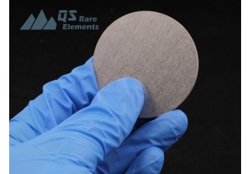
Tungsten Selenide (WSe2) Sputtering Targets
Composition: Tungsten Selenide (WSe2)
Catalog No.DPSE74ST
Purity:99.9% ~ 99.999%Please click ![]() for discount and other size
for discount and other size
- Product Details
Tungsten Selenide (WSe2) sputtering target specifications
Formula: WSe2
CAS No.: 12067-46-8
Max. dia. of flat disc sputter target: 10"
Typical lead time of WSe2 sputtering target:4 weeks
Regular Dimensions and Price of Tungsten Selenide (WSe2) Sputtering Target
| Product Name | Reference Price | |
| 2"diax 1/8"t Tungsten Selenide sputtering target | $714 | Add to Chart |
| 3"diax 1/8"t Tungsten Selenide sputtering target | $1500 | Add to Chart |
| 2"diax 1/8"t WSe2 sputtering target with In bonding to Cu bck plt | $794 | Add to Chart |
| 3"diax 1/8"t WSe2 sputtering target with In bonding to Cu bck plt | $1,635 | Add to Chart |
About Our Sputtering Target
QSAM is a professional supplier of custom manufacturered R&D consumptions. Our equipment setup are flexible to meet various demands from wide range of customers for flat disc sputter targets. We are supporting US national labs and worldwide univeristies and researching facilities with our target material and other customized product. Please check here for the list of our other Selenides sputter targets
About Tungsten Selenide
Tungsten selenide (WSe2) is a layered semiconductor belonging to the family of transition metal dichalcogenides (TMDs). It has a hexagonal crystal structure and exhibits unique electronic and optical properties. Thin films of WSe2 can be deposited using sputtering techniques, allowing for the fabrication of high-quality and uniform layers. Sputtered WSe2 films have garnered significant attention for their potential applications in optoelectronics and electronics. The layered nature of WSe2 enables the formation of atomically thin films with excellent carrier mobility and strong light-matter interactions. These properties make WSe2 suitable for the development of high-performance photodetectors, light-emitting diodes (LEDs), and transistors. Moreover, the ability to tune the electronic properties of WSe2 through layer thickness control and chemical doping has opened up new possibilities for the fabrication of novel electronic and optoelectronic devices. The deposition of WSe2 by sputtering has greatly advanced the study and application of this fascinating material in various technological fields.;
Tungsten Selenide Sputtering Target Packaging
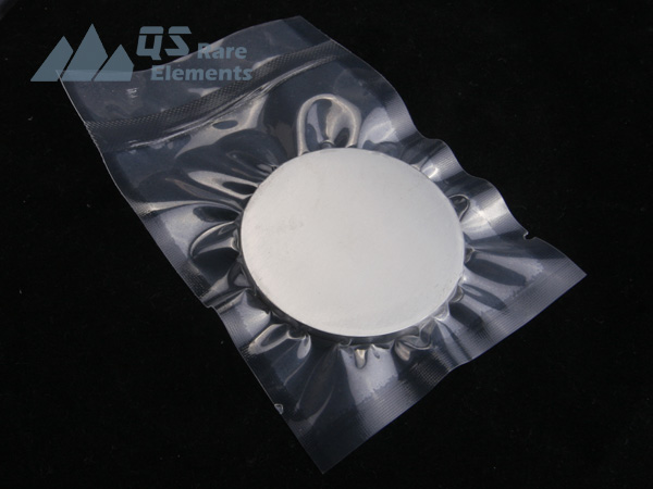
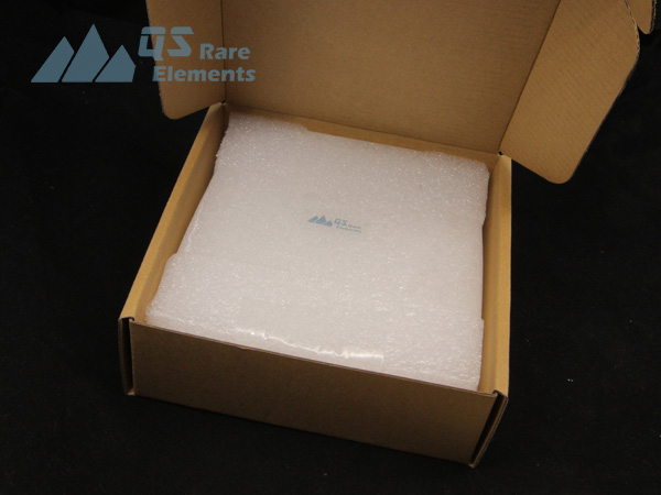
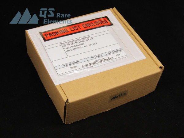
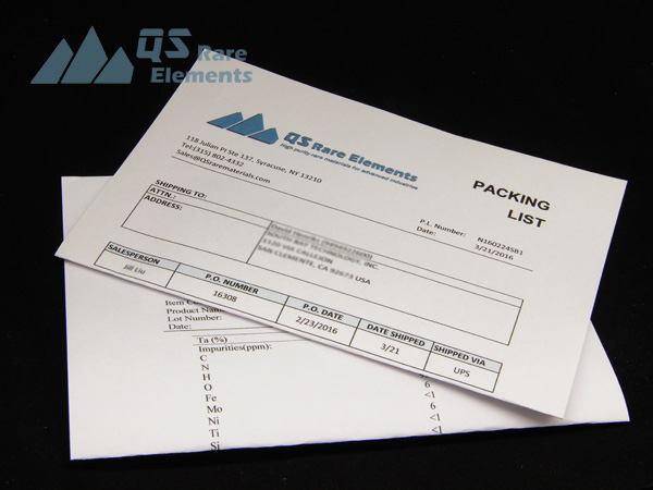
QSAMs sputter targets are vacuum sealed in plastic bags for shipping. We also use heavy foam to protect it. Common documents together with the sputter targets are packing list and analytical report e.g. COA
Related Product

